| CPC H10K 50/115 (2023.02) [H10K 50/15 (2023.02); H10K 50/16 (2023.02); H10K 50/818 (2023.02); H10K 50/828 (2023.02)] | 20 Claims |
|
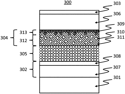
1. A light emitting device comprising:
a first electrode;
a second electrode; and
an emissive layer (EML) between the first electrode and the second electrode and electrically connected to the first electrode and the second electrode, the EML comprising:
a charge transport matrix of a first polarity;
a plurality of quantum dots in the charge transport matrix; and
a plurality of charge transport nanoparticles of a second polarity dispersed in the charge transport matrix, wherein
the EML is phase-separated into a lower emitting layer closer to the first electrode than the second electrode and an upper emitting layer closer to the second electrode than the first electrode, and
the lower emitting layer comprises higher in quantity of the plurality of charge transport nanoparticles than the quantity of charge transport nanoparticles in the upper emitting layer, and the upper emitting layer comprises higher in quantity of the plurality of quantum dots than the quantity of quantum dots in the lower emitting layer.
|