US 11,730,004 B2
Solid-state imaging element and solid-state imaging apparatus
Yohei Hirose, Tokyo (JP); Iwao Yagi, Kanagawa (JP); Shintarou Hirata, Tokyo (JP); Hideaki Mogi, Kanagawa (JP); Masashi Bando, Kanagawa (JP); and Osamu Enoki, Kanagawa (JP)
Assigned to SONY GROUP CORPORATION, Tokyo (JP); and SONY SEMICONDUCTOR SOLUTIONS CORPORATION, Kanagawa (JP)
Filed by SONY GROUP CORPORATION, Tokyo (JP); and SONY SEMICONDUCTOR SOLUTIONS CORPORATION, Kanagawa (JP)
Filed on Sep. 17, 2021, as Appl. No. 17/478,715.
Application 17/478,715 is a division of application No. 16/316,999, granted, now 11,158,675, previously published as PCT/JP2017/026243, filed on Jul. 20, 2017.
Claims priority of application No. 2016-142154 (JP), filed on Jul. 20, 2016; and application No. 2016-155728 (JP), filed on Aug. 8, 2016.
Prior Publication US 2022/0013584 A1, Jan. 13, 2022
Int. Cl. H01L 51/42 (2006.01); H10K 39/32 (2023.01); H04N 25/70 (2023.01); H10K 30/82 (2023.01); H10K 30/30 (2023.01); H10K 102/00 (2023.01)
CPC H10K 39/32 (2023.02) [H04N 25/70 (2023.01); H10K 30/353 (2023.02); H10K 30/82 (2023.02); H10K 2102/351 (2023.02)] 9 Claims
OG exemplary drawing
 
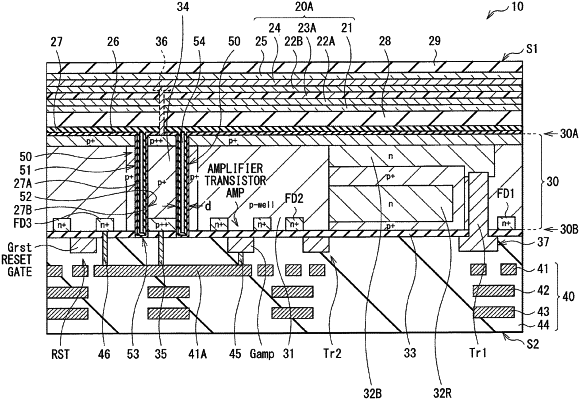
1. A solid-state imaging element comprising:
a first electrode;
a second electrode opposed to the first electrode; and
a photoelectric conversion layer provided between the first electrode and the second electrode, wherein
the photoelectric conversion layer includes an exciton generation layer including a dye material and a first semiconductor material, and an exciton disassociation layer including a second semiconductor material.