| CPC H10K 19/20 (2023.02) [H01L 33/0075 (2013.01); H01L 33/32 (2013.01); H10K 59/122 (2023.02); H10K 71/00 (2023.02)] | 20 Claims |
|
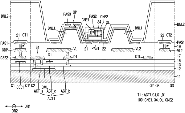
1. A display device comprising:
a first bank and a second bank spaced apart from each other and disposed on a substrate;
at least one semiconductor layer disposed between the first bank and the second bank;
a first electrode disposed on the first bank and electrically connected to a part of the at least one semiconductor layer;
an organic functional layer disposed on another part of the at least one semiconductor layer and comprising an organic light emitting layer; and
a second electrode disposed on the organic functional layer.
|