| CPC H10B 69/00 (2023.02) [B01J 37/16 (2013.01); C01G 3/00 (2013.01); C07C 1/12 (2013.01); C22B 15/00 (2013.01); C25B 3/25 (2021.01); C25B 11/051 (2021.01); C25B 11/075 (2021.01); C30B 7/14 (2013.01); C30B 29/02 (2013.01); C30B 29/64 (2013.01); G11C 16/04 (2013.01); H01L 23/528 (2013.01); H10B 41/27 (2023.02); H10B 41/30 (2023.02); H10B 43/00 (2023.02); H10B 43/20 (2023.02); H10B 43/30 (2023.02); C07C 2523/72 (2013.01)] | 8 Claims |
|
1. A process for forming a memory structure, comprising:
providing a semiconductor substrate having a planar surface;
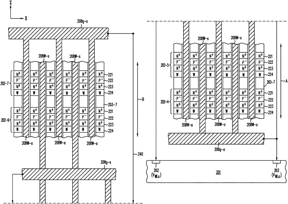
forming a first memory module above the planar surface, such that the first memory module includes a 3-dimensional array of NOR-type memory strings that comprises a plurality of NOR-type memory strings, with (i) two or more of the NOR-type memory strings being separated from each other along a first direction that is substantially parallel the planar surface and two or more of the NOR-type memory strings being separated from each other along a second direction that is orthogonal to the first direction and substantially perpendicular the planar surface, (ii) each of the NOR-type memory strings comprising a plurality of thin-film storage transistors, and (iii) a set of local word line conductors, each running along the second direction to serve as gate electrodes to the thin-film storage transistors of one or more of the NOR-type memory strings;
forming a first set of global conductors, such that the global conductors are (i) spaced from each other along a third direction that is substantially orthogonal both the first and second directions and (ii) each running along the first direction, in direct contact with selected local word line conductors of the first memory module;
forming a second memory module above the first memory module and the first set of global conductors, such that the second memory module also includes a 3-dimensional array of NOR-type memory strings that comprises a plurality of NOR-type memory strings, with (i) two or more of the NOR-type memory strings being separated from each other along the first direction and two or more of the NOR-type memory strings being separated from each other along the second direction, (ii) each of the NOR-type memory strings comprising a plurality of thin-film storage transistors, and (iii) a set of local word line conductors, each running along the second direction to serve as gate electrodes to the thin-film storage transistors of one or more of the NOR-type memory strings, and such that the first set of global conductors are also each in direct contact with selected local word line conductors of the second memory module.
|