| CPC H10B 63/84 (2023.02) [G11C 5/06 (2013.01); G11C 13/0002 (2013.01); H10N 70/826 (2023.02)] | 4 Claims |
|
1. An electronic device comprising a semiconductor memory, the semiconductor memory comprising:
a substrate having a substantially horizontal upper surface;
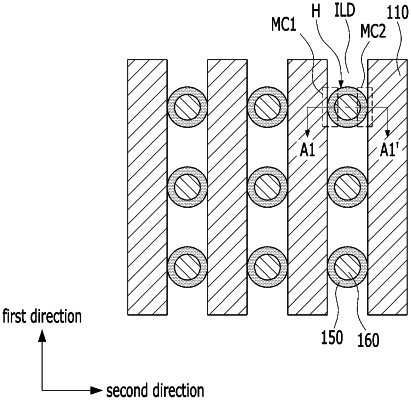
first to Nth layers (where N is a natural number of two or more) disposed in horizontal layers on the substrate and spaced apart from each other above the substrate in a vertical direction, wherein each of the first to Nth layers includes a plurality of conductive lines;
an insulating layer disposed to fill spaces between the conductive lines vertically;
a hole having sidewalls that extends in the vertical direction through the conductive lines of the first to Nth layers and the insulating layer therebetween;
a variable resistance layer disposed on the sidewalls of the hole; and
a conductive pillar disposed to fill the hole in which the variable resistance layer is formed.
|