| CPC H10B 53/30 (2023.02) [G11C 11/24 (2013.01); H10B 53/40 (2023.02); G11C 11/404 (2013.01); G11C 11/405 (2013.01)] | 20 Claims |
|
15. A system comprising:
a processor circuitry to execute one or more instructions;
a memory coupled to the processor circuitry; and
a communication interface to allow the processor circuitry to communicate with another device, wherein the memory includes a bit-cell which comprises:
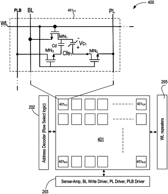
a node;
a first capacitor comprising non-linear polar material, the first capacitor having a first terminal coupled to the node and a second terminal coupled to a first plate-line;
a second capacitor comprising the non-linear polar material, the second capacitor having a third terminal coupled to the node and a fourth terminal coupled to a second plate-line;
a transistor coupled to the node and a bit-line, wherein the transistor is controllable by a word-line; and
a third capacitor coupled to the node and a third plate-line, wherein the second capacitor comprises a linear dielectric.
|