| CPC H10B 51/20 (2023.02) [H01L 29/24 (2013.01); H10B 51/10 (2023.02); H10B 51/30 (2023.02)] | 20 Claims |
|
1. A memory device, comprising:
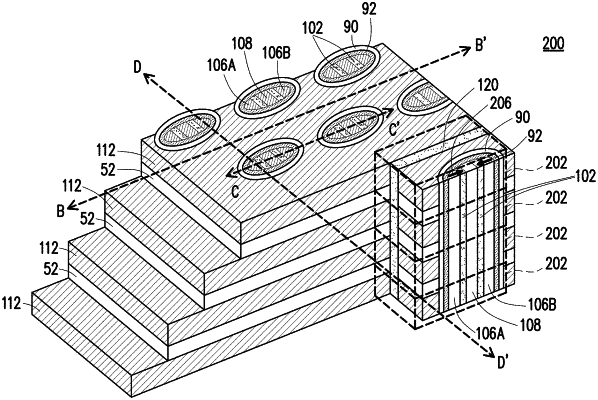
a multi-layer stack, disposed on a substrate and comprising a plurality of conductive layers and a plurality of dielectric layers stacked alternately along a first direction;
a channel layer, penetrating through the plurality of conductive layers and the plurality of dielectric layers;
a memory material layer, disposed between the channel layer and each of the plurality of conductive layers and the plurality of dielectric layers; and
at least three conductive pillars, extending in the first direction, surrounded by the channel layer and the memory material layer, wherein the at least three conductive pillars are electrically connected to conductive lines respectively, and the at least three conductive pillars are aligned along a second direction substantially perpendicular to the first direction.
|