| CPC H10B 51/20 (2023.02) [G11C 11/223 (2013.01); H01L 27/1225 (2013.01); H01L 29/66742 (2013.01); H01L 29/7869 (2013.01)] | 20 Claims |
|
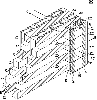
1. A memory cell comprising:
a thin film transistor over a semiconductor substrate, the thin film transistor comprising:
a memory film contacting a word line; and
an oxide semiconductor (OS) layer contacting a source line and a bit line, wherein the memory film is disposed between the OS layer and the word line, wherein the source line and the bit line are each physically separated from the memory film by the OS layer, wherein the source line and the bit line each comprise a first conductive material touching the OS layer, and wherein the first conductive material has a work function less than 4.6; and
a dielectric material separating the source line and the bit line.
|