| CPC H10B 43/50 (2023.02) [H10B 43/10 (2023.02); H10B 43/27 (2023.02)] | 19 Claims |
|
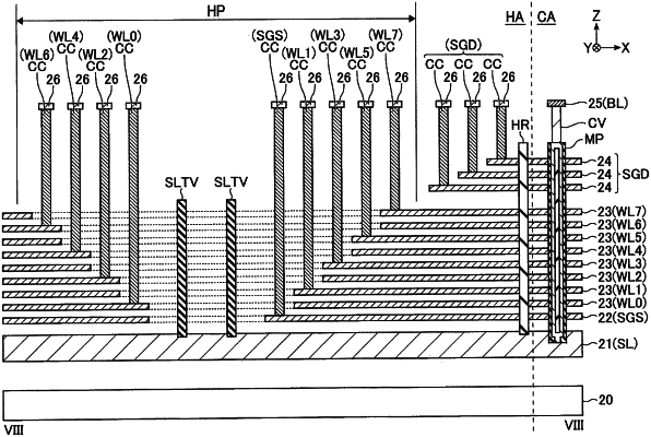
1. A semiconductor memory device comprising:
a first area and a second area arranged in a first direction;
a plurality of conductive layers arranged in a second direction intersecting the first direction, with first insulating layers each interposed between adjacent two of the conductive layers;
a first member and a second member arranged in a third direction intersecting each of the first direction and the second direction, the first member and the second member extending in the first direction across the first area and the second area and dividing the conductive layers;
a plurality of pillars penetrating the conductive layers in the first area;
a third member and a fourth member arranged in the third direction, the third member and the fourth member extending in the first direction and penetrating the conductive layers in the second area and between the first member and the second member, and
a fifth member extending in the first direction across the first area and the second area between the first member and the second member and dividing the conductive layers,
wherein:
an intersection of each of the pillars and each of the conductive layers in the first area functions as a memory cell;
the second area includes a first contact area including a first sub-area, a second sub-area, and a third sub-area, which are arranged in the first direction and interposed between the third member and the fourth member in the third direction;
the conductive layers include a first conductive layer, a second conductive layer, a third conductive layer, and a fourth conductive layer, which are arranged in order from bottom to top;
the first conductive layer includes a first terrace portion that does not overlap conductive layers above the first conductive layer of the conductive layers in the first sub-area;
the second conductive layer includes a second terrace portion that does not overlap conductive layers above the second conductive layer of the conductive layers in the third sub-area;
the third conductive layer includes a third terrace portion that does not overlap conductive layers above the third conductive layer of the conductive layers in the first sub-area;
the fourth conductive layer includes a fourth terrace portion that does not overlap conductive layers above the fourth conductive layer of the conductive layers in the third sub-area;
at least one contact extends in the second direction from each of the first to fourth terrace portions;
a part of the first sub-area of the conductive layers and a part of the third sub-area of the conductive layers are separated with the second sub-area interposed therebetween, and
the fifth member is arranged between the third member and the fourth member in the first contact area.
|
|
14. A semiconductor memory device comprising:
a first area and a second area arranged in a first direction;
a plurality of conductive layers arranged in a second direction intersecting the first direction, with first insulating layers each interposed between adjacent two of the conductive layers;
a first member and a second member arranged in a third direction intersecting each of the first direction and the second direction, the first member and the second member extending in the first direction across the first area and the second area and dividing the conductive layers;
a plurality of pillars penetrating the conductive layers in the first area;
a third member and a fourth member arranged in the third direction, the third member and the fourth member extending in the first direction and penetrating the conductive layers in the second area and between the first member and the second member; and
an eighth member and a ninth member arranged in the third direction and separated from the third member and the fourth member, the eighth member and the ninth member extending in the first direction and penetrating the conductive layers in the second area and between the first member and the second member,
wherein:
an intersection of each of the pillars and each of the conductive layers in the first area functions as a memory cell;
the second area includes a first contact area including a first sub-area, a second sub-area, and a third sub-area, which are arranged in the first direction and interposed between the third member and the fourth member in the third direction;
the conductive layers include a first conductive layer, a second conductive layer, a third conductive layer, and a fourth conductive layer, which are arranged in order from bottom to top;
the first conductive layer includes a first terrace portion that does not overlap conductive layers above the first conductive layer of the conductive layers in the first sub-area;
the second conductive layer includes a second terrace portion that does not overlap conductive layers above the second conductive layer of the conductive layers in the third sub-area;
the third conductive layer includes a third terrace portion that does not overlap conductive layers above the third conductive layer of the conductive layers in the first sub-area;
the fourth conductive layer includes a fourth terrace portion that does not overlap conductive layers above the fourth conductive layer of the conductive layers in the third sub-area;
at least one contact extends in the second direction from each of the first to fourth terrace portions;
a part of the first sub-area of the conductive layers and a part of the third sub-area of the conductive layers are separated with the second sub-area interposed therebetween;
the second area includes a second contact area including a fourth sub-area, a fifth sub-area, and a sixth sub-area, which are arranged in the first direction and interposed between the eighth member and the ninth member, the second contact area being separated from the first contact area;
the conductive layers include a fifth conductive layer, a sixth conductive layer, a seventh conductive layer, and an eighth conductive layer, which are arranged in order from bottom to top;
the fifth conductive layer includes a fifth terrace portion that does not overlap conductive layers above the fifth conductive layer of the conductive layers in the fourth sub-area;
the sixth conductive layer includes a sixth terrace portion that does not overlap conductive layers above the sixth conductive layer of the conductive layers in the sixth sub-area;
the seventh conductive layer includes a seventh terrace portion that does not overlap conductive layers above the seventh conductive layer of the conductive layers in the fourth sub-area;
the eighth conductive layer includes an eighth terrace portion that does not overlap conductive layers above the eighth conductive layer of the conductive layers in the sixth sub-area;
at least one contact extends in the second direction from each of the fifth to eighth terrace portions; and
a part of the fourth sub-area of the conductive layers and a part of the sixth sub-area of the conductive layers are separated with the fifth sub-area interposed therebetween.
|