US 11,729,984 B2
Semiconductor device and manufacturing method of semiconductor device
Jin Ha Kim, Icheon-si (KR)
Assigned to SK hynix Inc., Icheon-si (KR)
Filed by SK hynix Inc., Icheon-si (KR)
Filed on Aug. 3, 2022, as Appl. No. 17/880,002.
Application 17/880,002 is a continuation of application No. 16/847,251, filed on Apr. 13, 2020, granted, now 11,444,096.
Claims priority of application No. 10-2019-0146502 (KR), filed on Nov. 15, 2019.
Prior Publication US 2022/0375957 A1, Nov. 24, 2022
Int. Cl. H01L 27/11582 (2017.01); H01L 27/11548 (2017.01); H01L 27/11575 (2017.01); H10B 43/27 (2023.01); H10B 43/40 (2023.01); H01L 23/528 (2006.01); H10B 41/27 (2023.01); H10B 41/40 (2023.01); H10B 41/50 (2023.01); H10B 43/50 (2023.01)
CPC H10B 43/40 (2023.02) [H01L 23/528 (2013.01); H10B 41/27 (2023.02); H10B 41/40 (2023.02); H10B 41/50 (2023.02); H10B 43/27 (2023.02); H10B 43/50 (2023.02)] 18 Claims
OG exemplary drawing
 
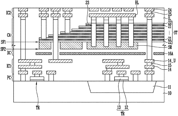
1. A method of manufacturing a semiconductor device, the method comprising:
forming a peripheral circuit;
forming a first interconnection structure that is electrically coupled to the peripheral circuit;
forming a decoupling structure having an electrically floating state over the first interconnection structure; and
forming a cell array over the decoupling structure.