| CPC H10B 43/27 (2023.02) [H01L 21/7682 (2013.01); H01L 21/76802 (2013.01); H01L 23/562 (2013.01); H10B 43/20 (2023.02); G11C 16/0466 (2013.01); H01L 21/31111 (2013.01)] | 19 Claims |
|
1. A memory structure, comprising:
a semiconductor substrate having a substantially planar surface;
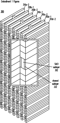
a first stack of active strips and a second stack of active strips formed over the surface of the semiconductor substrate and separated by a predetermined distance along a first direction substantially parallel the planar surface, wherein each stack of active strips comprises two or more active strips provided one on top of another, with adjacent active strips being isolated from each other by an isolation layer, the active strips being substantially aligned lengthwise with each other along a second direction that is substantially also parallel to the planar surface but orthogonal the first direction, and wherein each active strip comprises a dielectric layer provided between a conductive common source layer and a conductive common drain layer, and a channel layer in contact with both the common source layer and the common drain layer, the dielectric layer, the common source layer and the common drain layer being stacked along a third direction that is substantially normal to the planar surface;
a storage layer; and
a plurality of conductors, serving as gate electrodes, each extending lengthwise along the third direction, each conductor being within a group of the conductors that are provided between the first stack of active strips and the second stack of active strips and separated from each stack of active strips by the storage layer and the channel layer, thereby forming in each active strip at least one NOR string, each NOR string including a plurality of storage transistors that are formed out of the common source layer, the common drain layer, the channel layer and their adjacent storage layer and the conductors within the group.
|