| CPC H10B 43/27 (2023.02) [H10B 41/10 (2023.02); H10B 41/27 (2023.02); H10B 41/35 (2023.02); H10B 43/10 (2023.02); H10B 43/35 (2023.02)] | 7 Claims |
|
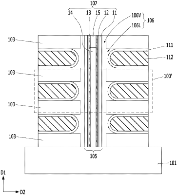
1. A memory device comprising:
an alternating stack of conductive layers and dielectric layers located over a substrate;
a vertical channel structure that penetrates the alternating stack;
a covering blocking layer that surrounds an outer wall of the vertical channel structure; and
a protruding blocking layer that extends from the covering blocking layer and contacts edges of the conductive layers,
wherein each of the conductive layers comprises a round-like edge contacting the protruding blocking layer,
wherein the protruding blocking layer contacts the dielectric layers, and comprises interface portions having cusp shapes and a middle portion between the interface portions, and
wherein each of the interface portions comprises oxide of porous nitride.
|