| CPC H10B 43/27 (2023.02) [G11C 16/0483 (2013.01); G11C 16/08 (2013.01); H01L 23/528 (2013.01); H01L 25/18 (2013.01); H01L 25/50 (2013.01); H01L 29/1037 (2013.01); H01L 29/7827 (2013.01); H10B 43/40 (2023.02)] | 20 Claims |
|
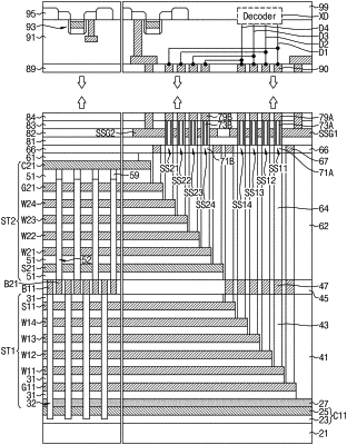
1. A semiconductor device, comprising:
a first stack structure including an alternating stack of a plurality of first word lines and a plurality of first insulating layers;
a plurality of first channel structures extending through the first stack structure;
a second stack structure on the first stack structure, the second stack structure including an alternating stack of a plurality of second word lines and a plurality of second insulating layers;
a plurality of second channel structures extending through the second stack structure, each of the plurality of second channel structures being offset from each of the plurality of first channel structures;
a plurality of first selectors connected to the plurality of first word lines;
a plurality of second selectors connected to the plurality of second word lines;
a plurality of first conductive pads disposed on the second stack structure, each of the plurality of first conductive pads being connected to a corresponding one of the plurality of first selectors and the plurality of second selectors;
a plurality of second conductive pads disposed on the plurality of first conductive pads, each of the plurality of second conductive pads being in direct contact with a corresponding one of the plurality of first conductive pads; and
a decoder disposed on the plurality of second conductive pads and connected to the plurality of second conductive pads.
|