| CPC H10B 43/27 (2023.02) [G11C 7/18 (2013.01); G11C 8/14 (2013.01); H10B 43/35 (2023.02)] | 12 Claims |
|
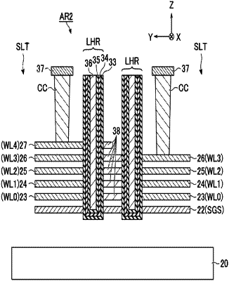
1. A semiconductor memory comprising:
a stack comprising a first region and a second region different from the first region, the first region including a plurality of first conductors and a plurality of first insulators alternately stacked in a first direction;
a first insulator portion and a second insulator portion respectively extending within the second region in the first direction and a second direction crossing the first direction, the first and second insulating portions being arranged in a third direction crossing the first and second directions; and
a plurality of layers provided between the first insulator portion and the second insulator portion, each of the plurality of layers being between adjacent two of the plurality of first insulators, a material of the plurality of layers being different from a material of the plurality of first conductors.
|