| CPC H10B 43/27 (2023.02) [G11C 7/18 (2013.01); G11C 8/14 (2013.01); H10B 41/10 (2023.02); H10B 41/27 (2023.02); H10B 41/35 (2023.02); H10B 43/10 (2023.02); H10B 43/35 (2023.02)] | 20 Claims |
|
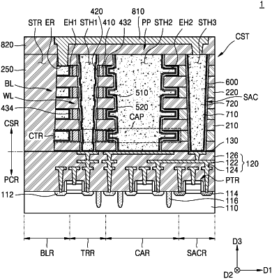
1. A semiconductor memory device comprising:
a word line extending in a vertical direction on a substrate;
a channel layer surrounding the word line to configure a cell transistor and having a horizontal ring shape with a predetermined horizontal width;
a bit line disposed at one end of the channel layer in a first horizontal direction and extending in a second horizontal direction perpendicular to the first horizontal direction; and
a cell capacitor disposed at other end of the channel layer in the first horizontal direction, the cell capacitor including an upper electrode layer extending in the vertical direction, a lower electrode layer surrounding the upper electrode layer, and a capacitor dielectric layer disposed between the upper electrode layer and the lower electrode layer.
|