| CPC H10B 43/27 (2023.02) [G11C 7/18 (2013.01); G11C 8/14 (2013.01); H01L 29/4234 (2013.01); H01L 29/7926 (2013.01); H10B 43/10 (2023.02); H01L 29/40117 (2019.08)] | 20 Claims |
|
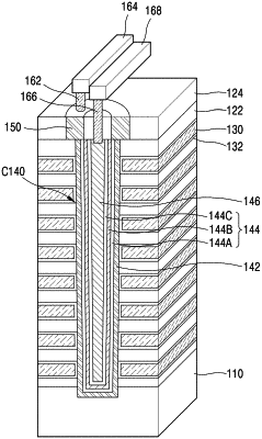
1. A semiconductor device comprising:
a channel structure on a substrate and extending in a first direction perpendicular to a top surface of the substrate, the channel structure comprising
a body gate layer extending in the first direction;
a charge storage structure surrounding a sidewall of the body gate layer; and
a channel layer surrounding a sidewall of the charge storage structure, an upper surface of the charge storage structure and an upper surface of the channel layer are at a same level;
a plurality of gate electrodes on the substrate and spaced apart from one another in the first direction on a sidewall of the channel structure; and
a gate insulating layer between each of the plurality of gate electrodes and the channel structure; and
a body gate contact contacting the body gate layer; and
a bit line contact being in electrical contact with the channel layer.
|