| CPC H10B 12/315 (2023.02) [G11C 5/063 (2013.01); H01L 29/0649 (2013.01); H10B 12/0335 (2023.02); H10B 12/05 (2023.02); H10B 12/482 (2023.02)] | 20 Claims |
|
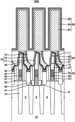
1. A method of forming a DRAM device, the method comprising:
forming an isolation region in a substrate, the isolation region defining a source region and a drain region;
recessing an upper surface of the source region to form a contact recess;
forming a bit line structure on the source region;
forming an inner spacer on a first sidewall of the bit line structure;
forming a sacrificial spacer on the inner spacer;
forming an outer spacer on the sacrificial spacer, wherein the sacrificial spacer is interposed between the inner spacer and the outer spacer;
forming a storage contact and a contact buffer layer on the drain region;
forming a capping spacer on the inner spacer, the sacrificial spacer, and the outer spacer;
conformally forming a landing pad barrier layer on the contact buffer layer and the capping spacer;
forming a landing pad on the landing pad barrier layer;
forming a trench between the landing pad and the bit line structure to expose a top portion of the sacrificial spacer;
removing the sacrificial spacer through the trench to form an air gap;
forming a first sealing layer on a first sidewall of the trench to seal a top of the air gap;
forming a second sealing layer on a second sidewall of the trench;
forming a pad isolation insulator between the first sealing layer and the second sealing layer to fill the trench; and
forming a storage structure on the landing pad.
|