| CPC H10B 12/30 (2023.02) [H01L 21/02266 (2013.01); H01L 21/02274 (2013.01); H01L 21/31116 (2013.01); H01L 21/3212 (2013.01); H01L 23/5329 (2013.01); H10B 12/02 (2023.02)] | 14 Claims |
|
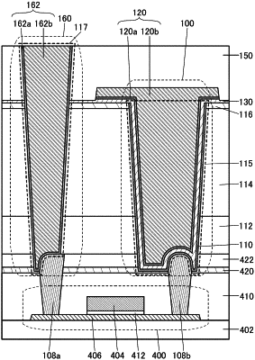
1. A semiconductor device comprising:
a semiconductor layer;
a first insulator comprising a depressed portion over the semiconductor layer;
a first conductor electrically connected to the semiconductor layer, the first conductor penetrating the first insulator;
a second insulator over the first insulator, the second insulator comprising an opening overlapping with the depressed portion and the first conductor; and
a second conductor in direct contact with the depressed portion, a curved surface of the first conductor, and an inner wall of the opening,
wherein the first conductor penetrates the second insulator, and
wherein the first conductor comprises the curved surface in a portion above a top surface of the first insulator.
|
|
2. A semiconductor device comprising:
a semiconductor layer;
a first insulator comprising a depressed portion over the semiconductor layer;
a first conductor electrically connected to the semiconductor layer, the first conductor penetrating the first insulator;
a second insulator over the first insulator, the second insulator comprising an opening overlapping with the depressed portion and the first conductor;
a second conductor in direct contact with the depressed portion, a curved surface of the first conductor, and an inner wall of the opening;
a third insulator over the second conductor and in the opening; and
a third conductor over the third insulator,
wherein the third conductor overlaps with the semiconductor layer, and
wherein the first conductor comprises the curved surface in a portion above a top surface of the first insulator.
|