| CPC H10B 12/30 (2023.02) [H01L 29/4236 (2013.01)] | 17 Claims |
|
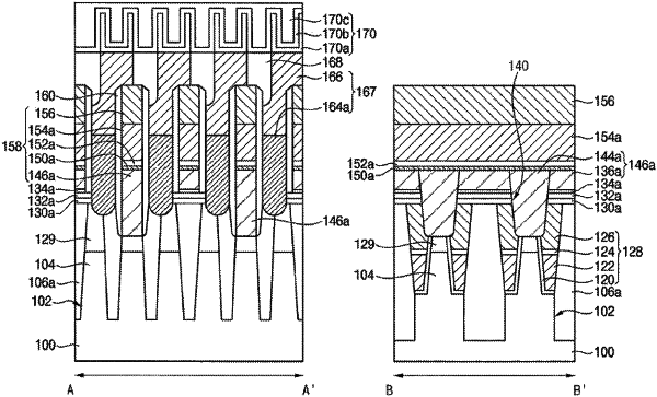
1. A semiconductor device, comprising:
a substrate including an isolation layer pattern and an active pattern;
a buffer insulation layer pattern on the substrate;
a polysilicon structure on the active pattern and the buffer insulation layer pattern, the polysilicon structure contacting a portion of the active pattern, and the polysilicon structure extending in a direction parallel to an upper surface of the substrate;
a first diffusion barrier layer pattern on an upper surface of the polysilicon structure, the first diffusion barrier layer pattern including polysilicon doped with at least carbon;
a second diffusion barrier layer pattern on the first diffusion barrier layer pattern, the second diffusion barrier layer pattern including at least a metal; and
a first metal pattern and a first capping layer pattern stacked on the second diffusion barrier layer pattern.
|