| CPC H10B 12/00 (2023.02) [G11C 5/02 (2013.01); G11C 11/403 (2013.01); G11C 11/409 (2013.01); H01L 29/24 (2013.01)] | 14 Claims |
|
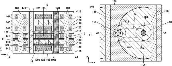
1. A semiconductor device comprising:
a substrate;
a first oxide layer over the substrate, the first oxide layer comprising a first region, a second region, and a third region positioned between the first region and the second region;
a second oxide layer comprising In and Zn;
a first conductive layer overlapping with the first oxide layer;
a first insulating layer overlapping and being in contact with the first oxide layer and the first conductive layer and surrounding the second oxide layer;
a third oxide layer over the first conductive layer;
a second conductive layer overlapping with the third oxide layer; and
a second insulating layer overlapping and being in contact with the third oxide layer and the second conductive layer and surrounding the second oxide layer,
wherein each of the first region and the second region has a lower resistance than the third region.
|