| CPC H05K 9/0022 (2013.01) [H05K 7/20454 (2013.01); H05K 7/20509 (2013.01); H05K 9/009 (2013.01); H05K 9/0088 (2013.01)] | 19 Claims |
|
1. An electronic device comprising:
a printed circuit board;
at least one electronic component mounted on the printed circuit board; and
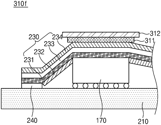
a shielding film including a conductive layer and an insulation layer, the shielding film attached to at least a part of the printed circuit board and contacting an upper side surface of the at least one electronic component,
wherein the conductive layer includes a nano-conductive fiber and is electrically connected with a first ground part of the printed circuit board through the nano-conductive fiber,
wherein the insulation layer defines a hole, and
wherein a position of the hole corresponds to a position of the at least one electronic component, such that an upper side surface of the at least one electronic component directly contacts the conductive layer through the hole.
|