| CPC H05K 5/0217 (2013.01) [H05K 7/1427 (2013.01)] | 20 Claims |
|
1. A portable communication device comprising:
a display;
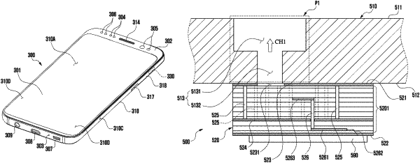
a housing accommodating the display, the housing comprising a side member, the side member comprising a conductive portion and a non-conductive portion, the conductive portion having an opening formed therein, the non-conductive portion being at least partially disposed in the opening, the opening being formed from an outer surface to an inner surface of the conductive portion such that, when viewed in a first direction perpendicular to the display, a first opening portion extending from the outer surface has a first length in a second direction, the second direction corresponding to an extending direction of a length of the conductive portion, and a second opening portion extending from and being connected to the first opening portion has a second length in the second direction smaller than the first length;
an antenna circuitry disposed parallel to the side member, the antenna circuitry comprising:
a printed circuit board comprising a first layer facing the side member and a second layer facing a direction opposite to that of the first layer,
a first portion disposed at the printed circuit board, the first portion including a radiating element facing the second opening portion and being disposed between the first layer and the second layer, the radiating element being connected to a feeding line through a conductive line extended in a direction perpendicular to each of the feeding line and the radiating element, and
a second portion adjacent to the first portion at the printed circuit board and facing a part of the conductive portion, the second portion including a plurality of conductive vias formed therein, at least one via of the plurality of conductive vias being electrically connected to a ground layer included in the printed circuit board; and
a communication circuit electrically connected to the antenna circuitry.
|