| CPC H05K 3/284 (2013.01) [H05K 1/0393 (2013.01); H05K 1/111 (2013.01); H05K 3/0067 (2013.01); H05K 3/1283 (2013.01); H05K 2203/1316 (2013.01); H05K 2203/1322 (2013.01)] | 25 Claims |
|
1. A method for manufacturing a number of electrical nodes, wherein the method comprises:
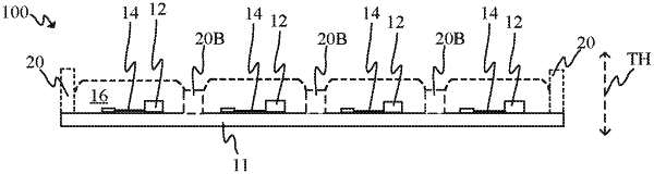
obtaining or providing a number of electronic circuits on or onto, respectively, a first substrate, wherein each one of the electronic circuits comprises a circuit pattern and at least one electronics component in connection with the circuit pattern, wherein the electronic circuits are spaced from each other on the first substrate, thereby defining a blank area surrounding each one of the number of electronic circuits, respectively, and
providing potting or casting material to embed each one of the number of electronic circuits in the potting or casting material, wherein the potting or casting material is a mixed two-component potting or casting material,
after embedding each one of the number of electronic circuits in the potting or casting material, pushing a roller or mold into the potting or casting material when the potting or casting material is in an unhardened state to create recesses in the potting or casting material at locations disposed between and offset from the electronic circuits for providing barrier or dam elements around the number of electronic circuits, and, subsequently,
hardening the potting or casting material to form a filler material layer of the number of electrical nodes at room temperature over time.
|