| CPC H05K 1/186 (2013.01) [H05K 1/113 (2013.01); H01G 4/33 (2013.01); H05K 2201/10015 (2013.01)] | 12 Claims |
|
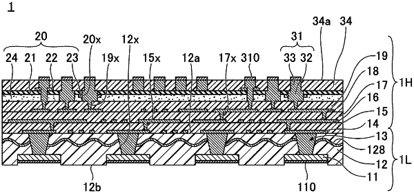
1. A wiring board comprising:
an insulating layer;
a thin film capacitor laminated on the insulating layer;
an interconnect layer electrically connected to the thin film capacitor; and
an encapsulating resin layer laminated on the thin film capacitor, wherein
the thin film capacitor includes a dielectric provided between the insulating layer and the encapsulating resin layer, a first electrode provided on a first surface of the dielectric, and a second electrode provided on a second surface of the dielectric opposite to the first surface,
the interconnect layer includes a first via interconnect electrically connected to the first electrode, a first pad formed continuously with the first via interconnect and protruding from the thin film capacitor, a second via interconnect electrically connected to the second electrode, and a second pad formed continuously with the second via interconnect and protruding from the thin film capacitor,
the first via interconnect penetrates the encapsulating resin layer, the first electrode, and the dielectric,
the second via interconnect penetrates the encapsulating resin layer, the dielectric, and the second electrode,
the encapsulating resin layer is a mold resin having a non-photosensitive thermosetting resin as a main component thereof, and
the encapsulating resin layer exposes a top surface of each of the first and second pads, and covers at least a portion of a side surface of each of the first and second pads.
|