| CPC H05K 1/0225 (2013.01) [G05B 19/4097 (2013.01); H05K 3/027 (2013.01); G05B 2219/45026 (2013.01); G05B 2219/45034 (2013.01); H05K 1/18 (2013.01); H05K 2201/093 (2013.01); H05K 2201/098 (2013.01); H05K 2201/09027 (2013.01); H05K 2201/10098 (2013.01)] | 13 Claims |
|
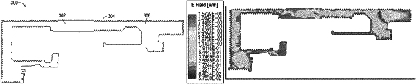
1. A circuit board for use in a wireless communication device comprising an antenna, the circuit board comprising: a power plane; and a ground plane,
the circuit board comprising a plurality of cuts at an edge of the power plane, each cut extending from the edge of the power plane to a point at a depth into the power plane, the plurality of cuts to control impedance at an edge of the circuit board to reduce radio-frequency (RF) emissions by the circuit board,
wherein the plurality of the cuts are provided along the edge of the power plane such that an impedance of the power plane at the depth of each cut is different than an impedance of the power plane at the edge of the power plane.
|