| CPC H05K 1/0225 (2013.01) [G01R 1/18 (2013.01); H05K 3/34 (2013.01); H05K 3/3447 (2013.01); H05K 9/0069 (2013.01); H05K 2203/1147 (2013.01); Y10T 29/49002 (2015.01); Y10T 29/49117 (2015.01)] | 10 Claims |
|
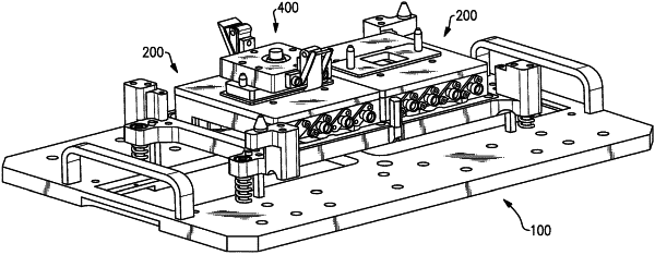
1. A method for shielding a printed circuit board from electromagnetic interference and noise during noise figure testing, comprising:
inserting a printed circuit board with at least one radiofrequency component mounted thereon through an opening in a cover of a cavity of a housing, the cavity defined by a peripheral wall of the housing;
attaching one or more radiofrequency connectors to the peripheral wall so that a pin of each radiofrequency connectors substantially aligns with an electrical contact on the printed circuit board;
soldering the pin of the one or more radiofrequency connectors to its corresponding electrical contact on the printed circuit board; and
sealing the opening in the cover of the housing with a tool to at least partially seal the cavity.
|