| CPC H04N 25/772 (2023.01) [H04N 25/57 (2023.01); H04N 25/709 (2023.01); H04N 25/75 (2023.01)] | 23 Claims |
|
1. An imaging device comprising:
a pixel circuit configured to output a pixel signal;
a pixel signal line coupled to the pixel circuit;
a reference signal generation circuit configured to output a reference signal; and
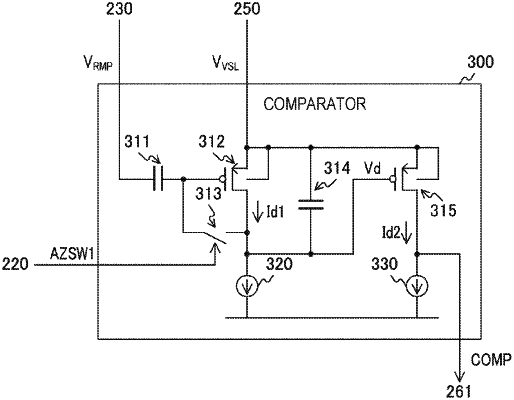
a comparator including:
a first transistor, wherein a gate of the first transistor is coupled to the reference signal generation circuit and a source of the first transistor is coupled to the pixel signal line, and
a second transistor, wherein a gate of the first second transistor is coupled to a drain of the first transistor and a source of the second transistor is electrically connected to the pixel signal line.
|