US 11,729,530 B2
Solid-state imaging device, method of manufacturing solid-state imaging device, and electronic apparatus
Hiroaki Ammo, Kanagawa (JP)
Assigned to SONY SEMICONDUCTOR SOLUTIONS CORPORATION, Kanagawa (JP)
Filed by SONY SEMICONDUCTOR SOLUTIONS CORPORATION, Kanagawa (JP)
Filed on May 3, 2022, as Appl. No. 17/735,246.
Application 17/735,246 is a continuation of application No. 17/315,014, filed on May 7, 2021, granted, now 11,343,455.
Application 17/315,014 is a continuation of application No. 16/844,670, filed on Apr. 9, 2020, granted, now 11,032,504, issued on Jun. 8, 2021.
Application 16/844,670 is a continuation of application No. 16/055,377, filed on Aug. 6, 2018, granted, now 10,645,321, issued on May 5, 2020.
Application 16/055,377 is a continuation of application No. 15/671,227, filed on Aug. 8, 2017, granted, now 10,044,962, issued on Aug. 7, 2018.
Application 15/671,227 is a continuation of application No. 15/146,099, filed on May 4, 2016, granted, now 9,762,832, issued on Sep. 12, 2017.
Application 15/146,099 is a continuation of application No. 14/363,971, granted, now 9,363,451, issued on Jun. 7, 2016, previously published as PCT/JP2012/081755, filed on Dec. 7, 2012.
Claims priority of application No. 2011-277076 (JP), filed on Dec. 19, 2011.
Prior Publication US 2022/0264040 A1, Aug. 18, 2022
This patent is subject to a terminal disclaimer.
Int. Cl. H04N 25/76 (2023.01); H01L 27/146 (2006.01); H04N 25/60 (2023.01); H04N 25/75 (2023.01); H04N 25/77 (2023.01)
CPC H04N 25/76 (2023.01) [H01L 27/14607 (2013.01); H01L 27/14614 (2013.01); H01L 27/14643 (2013.01); H04N 25/60 (2023.01); H04N 25/75 (2023.01); H04N 25/77 (2023.01); H01L 27/14689 (2013.01)] 16 Claims
OG exemplary drawing
 
1. A light detecting device, comprising:
a semiconductor layer including a first surface side and a second surface side, wherein the first surface side is opposite to the second surface side;
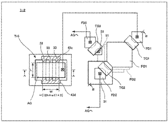
a first photoelectric conversion portion in the semiconductor layer;
a first transfer transistor at the first surface side;
a first floating diffusion region in the semiconductor layer; and
a pixel transistor below the first surface side, wherein
the pixel transistor includes a fin type gate electrode,
the first photoelectric conversion portion and the first transfer transistor are in a first region of the light detecting device, and
the pixel transistor is in a second region of the light detecting device.