| CPC H04N 25/75 (2023.01) [H01L 27/1461 (2013.01); H01L 27/1463 (2013.01); H01L 27/14612 (2013.01)] | 16 Claims |
|
1. A photosensitive array, comprising:
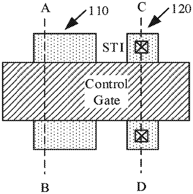
a substrate defining a plurality of pixel regions arranged in rows and columns and substrate tap regions scattered among the pixel regions, each pixel region comprising a photosensitive region for accommodating a MOS capacitor and a charge readout region for accommodating a readout transistor, each pixel region corresponding to one of the substrate tap regions, the substrate of the pixel region continuing with the substrate of the corresponding substrate tap region, the substrate tap region providing a voltage application location for the substrate of the corresponding pixel region, wherein the columns include sets of two adjacent columns, in each of which sets the charge readout regions of each column directly face the charge readout regions of the other column while the photosensitive regions of each column are separated from the photosensitive regions of the other column by the charge readout regions, and each of which sets includes subsets of four pixel regions belonging to two adjacent ones of the rows and surrounding a corresponding one of the substrate tap regions; and
isolation structures disposed in the substrate, the isolation structures including through trench isolations extending through the substrate along a thickness direction thereof, the through trench isolations extending laterally within the substrate to isolate adjacent pixel regions, the substrate of each pixel region continuing with the substrate of the corresponding substrate tap regions.
|