| CPC H04N 25/531 (2023.01) [H04N 25/533 (2023.01); H04N 25/58 (2023.01); H04N 25/75 (2023.01); H04N 25/766 (2023.01); H04N 25/77 (2023.01)] | 20 Claims |
|
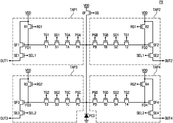
1. A depth sensor comprising:
a pixel including a first tap, a second tap, a third tap, a fourth tap, an overflow transistor, and a photoelectric conversion device, each tap of the first tap, the second tap, the third tap, and the fourth tap including a photo transistor, a transfer transistor, and a readout circuit; and
a row driver configured to control the pixel,
wherein the row driver is further configured to:
in a first integration period of a global mode, activate a second photo gate signal controlling the photo transistor of the second tap and a third photo gate signal controlling the photo transistor of the third tap; and
in a second integration period of the global mode, activate a first photo gate signal controlling the photo transistor of the first tap and a fourth photo gate signal controlling the photo transistor of the fourth tap.
|