US 11,729,496 B2
Imaging device, imaging system, and imaging method
Naoki Kawazu, Kanagawa (JP); Keita Sasaki, Kanagawa (JP); Takumi Oka, Kanagawa (JP); Yuichi Motohashi, Tokyo (JP); and Atsushi Suzuki, Kanagawa (JP)
Assigned to SONY SEMICONDUCTOR SOLUTIONS CORPORATION, Kanagawa (JP)
Filed by SONY SEMICONDUCTOR SOLUTIONS CORPORATION, Kanagawa (JP)
Filed on May 3, 2022, as Appl. No. 17/735,612.
Application 17/735,612 is a continuation of application No. 16/970,066, granted, now 11,343,427, previously published as PCT/JP2019/004036, filed on Feb. 5, 2019.
Claims priority of application No. 2018-029771 (JP), filed on Feb. 22, 2018.
Prior Publication US 2022/0279121 A1, Sep. 1, 2022
Int. Cl. H04N 5/232 (2006.01); H04N 5/235 (2006.01); H04N 5/369 (2011.01); H04N 5/367 (2011.01); H04N 5/378 (2011.01); H04N 23/65 (2023.01); H04N 23/70 (2023.01); H04N 25/75 (2023.01); H04N 25/79 (2023.01); H04N 25/683 (2023.01)
CPC H04N 23/65 (2023.01) [H04N 23/749 (2023.01); H04N 25/683 (2023.01); H04N 25/75 (2023.01); H04N 25/79 (2023.01)] 18 Claims
OG exemplary drawing
 
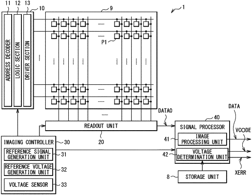
1. An imaging device, comprising:
a pixel array including a plurality of pixels, wherein each pixel of the plurality of pixels is configured to generate a pixel voltage;
a voltage sensor configured to generate a first detection voltage;
an AD converter coupled to the pixel array and the voltage sensor, wherein the AD converter is configured to generate first detection voltage data based on the first detection voltage; and
a flag generator configured to generate a first error flag based on the first detection voltage data and first reference voltage data, wherein
the first reference voltage data has a determined range, and
the first error flag is set to a ground voltage based on a determination that the first detection voltage data is outside the determined range.