| CPC H04L 7/0037 (2013.01) [H04L 7/033 (2013.01)] | 19 Claims |

|
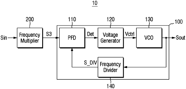
1. A clock generating circuit comprising:
a first frequency multiplier configured to generate a second clock signal having a second frequency based on a first clock signal having a first frequency; and
a second frequency multiplier configured to generate a third clock signal having a third frequency based on the second clock signal,
wherein the first frequency multiplier comprises:
a pulse width control circuit configured to control a duty cycle of the first clock signal;
a first delay circuit configured to receive the first clock signal of which the duty cycle has been controlled, and delay the received first clock signal based on a duty cycle of the second clock signal to output a first delay clock signal; and
a first exclusive OR gate configured to perform an exclusive OR computation on the first clock signal of which the duty cycle has been controlled and the first delay clock signal to output the second clock signal,
wherein the second frequency is greater than the first frequency, and the third frequency is greater than the second frequency,
wherein the first delay circuit receives a control signal based on a comparison signal output by the second frequency multiplier, the comparison signal including information on the duty cycle of the second clock signal.
|