| CPC H03L 7/1976 (2013.01) [H03L 7/087 (2013.01); H03L 7/0807 (2013.01); H03L 7/099 (2013.01); H04L 7/0331 (2013.01)] | 11 Claims |
|
1. A clock and data recovery (CDR) device, comprising:
a digital phase detector circuit configured to (i) receive a data signal and an output clock signal, (ii) detect a phase difference between the data signal and the output clock signal, and (iii) generate a phase difference signal based on the detected phase difference; and
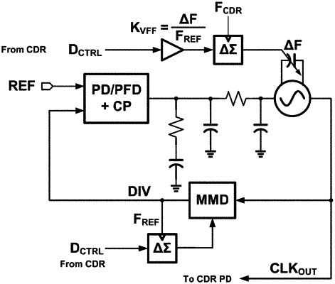
a fractional-N phase lock loop (Frac-N PLL) circuit configured to control either one of an output frequency and an output phase of the output clock signal according to a digital frequency control signal that is based on the detected phase difference between the data signal and the output clock signal, the Frac-N PLL circuit being configured to (i) receive the digital frequency control signal and a reference clock signal, the digital frequency control signal being indicative of the phase difference between the data signal and the output clock signal (ii) generate the output clock signal using an oscillator that is controlled in accordance with the digital frequency control signal and the reference clock signal,
wherein the Frac-N PLL circuit comprises a feedforward path circuit that includes a sigma delta modulator configured to generate an oscillator compensation signal based on the digital frequency control signal and a digital gain scaling factor.
|