| CPC H03K 17/04206 (2013.01) [H03K 17/04123 (2013.01); H03K 17/687 (2013.01); H03K 2217/0054 (2013.01)] | 18 Claims |
|
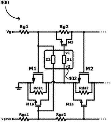
1. A radio frequency (RF) switch comprising:
a switchable RF path comprising a plurality of transistors coupled in series;
a gate bias network comprising a plurality of resistors, wherein the gate bias network is coupled to each of the plurality of transistors in the switchable RF path; and
a bypass network comprising a plurality of transistors coupled in parallel with each of the plurality of transistors in the switchable RF path and at least one additional transistor coupled in parallel with at least one resistor in the gate bias network,
wherein the at least one additional transistor is coupled to a first variable resistor, and wherein at least one resistor in the gate bias network is coupled to a second variable resistor.
|