| CPC H03H 3/02 (2013.01) [H03H 3/04 (2013.01); H03H 9/02118 (2013.01); H03H 9/0514 (2013.01); H03H 9/1035 (2013.01); H03H 9/131 (2013.01); H03H 9/132 (2013.01); H03H 9/133 (2013.01); H03H 9/171 (2013.01); H03H 9/174 (2013.01); H03H 9/564 (2013.01); H03H 9/568 (2013.01); H03H 2003/0414 (2013.01); H03H 2003/0428 (2013.01)] | 10 Claims |

|
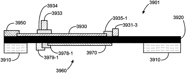
1. A method for fabricating an acoustic resonator device, the method comprising:
providing a substrate having a substrate surface region and a substrate backside cavity region characterized by a cavity geometric area;
forming a piezoelectric layer overlying the substrate surface region, the piezoelectric layer having a top piezoelectric surface region and a bottom piezoelectric surface region;
forming a backside energy confinement structure underlying the bottom piezoelectric surface region, the backside energy confinement structure being characterized by a backside structure geometric area and a backside structure perimeter, the backside energy confinement structure having at least one portion removed forming a backside structure break region; and
forming a backside metal electrode underlying the bottom piezoelectric surface region and within the backside energy confinement structure, the backside metal electrode being characterized by a backside electrode geometric area.
|