| CPC H03F 1/0216 (2013.01) [H03F 1/0227 (2013.01); H03F 1/0266 (2013.01); H03F 1/56 (2013.01); H03F 3/19 (2013.01); H03F 3/193 (2013.01); H03F 3/195 (2013.01); H03F 3/24 (2013.01); H03F 3/245 (2013.01); H04B 1/04 (2013.01); H01L 25/0655 (2013.01); H01L 2224/16227 (2013.01); H01L 2224/48227 (2013.01); H01L 2924/15313 (2013.01); H01L 2924/19041 (2013.01); H01L 2924/19042 (2013.01); H01L 2924/19043 (2013.01); H01L 2924/19105 (2013.01); H03F 1/302 (2013.01); H03F 3/04 (2013.01); H03F 3/191 (2013.01); H03F 2200/102 (2013.01); H03F 2200/105 (2013.01); H03F 2200/222 (2013.01); H03F 2200/318 (2013.01); H03F 2200/336 (2013.01); H03F 2200/451 (2013.01); H04B 1/3827 (2013.01); H04B 2001/045 (2013.01); H04B 2001/0416 (2013.01)] | 20 Claims |
|
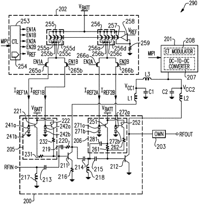
1. A mobile device comprising:
a power amplifier including an amplification transistor having an input configured to receive a radio frequency signal, a first bias network electrically connected to the input of the amplification transistor, and a second bias network electrically connected to the input of the amplification transistor;
a bias control circuit including a first switch, a first reference current source configured to provide a first reference current to the first bias network through the first switch, a second switch, and a second reference current source configured to provide a second reference current to the second bias network through the second switch; and
a power management circuit configured to control a voltage level of a supply voltage of the power amplifier, the power management circuit operable in a first mode and a second mode.
|