| CPC H01S 5/34333 (2013.01) [H01S 5/0206 (2013.01); H01S 5/0207 (2013.01); H01S 5/0208 (2013.01); H01S 5/04257 (2019.08); H01S 5/18361 (2013.01)] | 8 Claims |
|
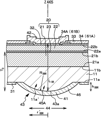
1. A light emitting element comprising:
a compound semiconductor substrate;
a stacked structure including a GaN-based compound semiconductor;
a first light reflection layer; and
a second light reflection layer,
wherein the stacked structure includes, in a stacked state
a first compound semiconductor layer that is formed on the compound semiconductor substrate and that has a first surface and a second surface opposite to the first surface,
an active layer facing the second surface of the first compound semiconductor layer, and
a second compound semiconductor layer that has a first surface facing the active layer and a second surface opposite to the first surface,
the first light reflection layer is disposed on the compound semiconductor substrate and has a concave mirror section,
the second light reflection layer is disposed on the second surface side of the second compound semiconductor layer and has a flat shape, and
the compound semiconductor substrate includes a low impurity concentration compound semiconductor substrate or a semi-insulating compound semiconductor substrate,
wherein the second compound semiconductor layer is provided with a current injection region and a current non-injection region surrounding the current injection region, and
a shortest distance DCI from an area center of gravity of the current injection region to a boundary between the current injection region and the current non-injection region satisfies the following formula:
DCI≥ω0/2
provided that
ω02≡(λ0/π){LOR(RDBR−LOR}1/2
where
λ0: wavelength of light mainly emitted from light emitting element
LOR: cavity length
RDBR: radius of curvature of concave mirror section of first light reflection layer.
|