| CPC H01Q 1/243 (2013.01) [H01Q 1/24 (2013.01); H01Q 1/245 (2013.01); H01Q 3/24 (2013.01); H01Q 3/247 (2013.01); H01Q 5/364 (2015.01); H01Q 9/42 (2013.01); H01Q 21/28 (2013.01); H01Q 1/48 (2013.01); H01Q 5/35 (2015.01); H01Q 7/00 (2013.01); H01Q 9/0421 (2013.01); H04M 1/0266 (2013.01)] | 20 Claims |
|
1. An electronic device, comprising:
a housing including a first surface, a second surface opposite to the first surface, and first to fourth side surfaces disposed between the first surface and the second surface;
a first conductive portion, a second conductive portion, a third conductive portion and a fourth conductive portion forming the first to third side surfaces;
a first nonconductive member exposed through the first side surface and separating the first conductive portion and the third conductive portion;
a second nonconductive member exposed through the second side surface and separating the first conductive portion and the second conductive portion;
a third nonconductive member exposed through the third side surface opposite to the first side surface and separating the second conductive portion and the fourth conductive portion;
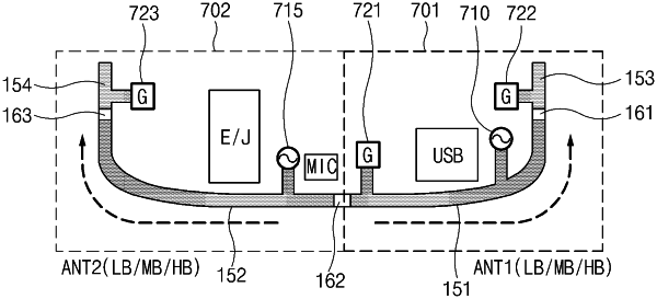
a first ground part electrically connected to the second conductive portion at a point adjacent to the third nonconductive member;
a second ground part electrically connected to the fourth conductive portion at a point adjacent to the third nonconductive member; and
a communication circuit electrically connected with at least one of the first conductive portion, the second conductive portion and the third conductive portion,
wherein the second conductive portion and the fourth conductive portion operate as a first antenna configured to transmit and receive a first multi-band frequency signal,
wherein the first conductive portion forms a first part of the first side surface and a first part of the second side surface,
wherein the second conductive portion forms at a second part of the second side surface and a first part of the third side surface,
wherein the third conductive portion forms a second part of the first side surface, and
wherein the fourth conductive portion forms a second part of the third side surface.
|