| CPC H01L 33/62 (2013.01) [H01L 33/0093 (2020.05); H01L 33/38 (2013.01); H01L 33/44 (2013.01); H01L 2933/0025 (2013.01); H01L 2933/0066 (2013.01)] | 14 Claims |
|
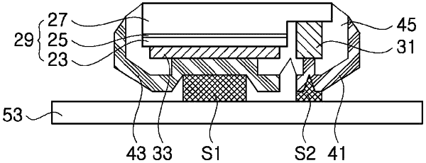
1. A display apparatus comprising a light emitting diode chip,
wherein:
the light emitting diode chip comprises:
a light emitting structure including a first conductivity type semiconductor layer, a second conductivity type semiconductor layer, and an active layer interposed between the first and second conductivity type semiconductor layers;
a first electrode electrically connected to the first conductivity type semiconductor layer;
a second electrode electrically connected to the second conductivity type semiconductor layer;
an insulator covering portions of upper surfaces of the first and second electrodes and portions of side surfaces of the light emitting structure; and
couplers disposed on the first and second electrodes and side surfaces of the light emitting structure;
the insulator is disposed between the couplers and the light emitting chip; and
the light emitting structure is separated from a growth substrate so that a bottom surface of the first conductivity type semiconductor layer is exposed.
|