| CPC H01L 33/24 (2013.01) [G02B 27/0172 (2013.01); G06F 1/163 (2013.01); H01L 25/0753 (2013.01); H01L 33/0062 (2013.01); H01L 33/60 (2013.01); H01L 33/62 (2013.01); G02B 2027/0178 (2013.01); H01L 2933/0058 (2013.01); H01L 2933/0066 (2013.01)] | 15 Claims |
|
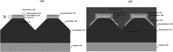
1. A method comprising:
forming a plurality of stacks on a surface of a semiconductor structure, wherein the semiconductor structure comprises a p-type layer, an active layer, and an n-type layer, and wherein each stack is a layered structure comprising a p contact located at an interface between the stack and the p-type layer of the semiconductor structure;
etching the semiconductor structure to form a plurality of mesa shapes using the stacks as etch masks, such that each mesa shape is formed beneath a corresponding stack;
forming a dielectric on at least a portion of each mesa shape and at least a portion of each stack; and
forming a reflector on at least a portion of the dielectric and at least a portion of the semiconductor structure, wherein:
an interface between the reflector and the n-type layer of the semiconductor structure forms an n contact, and
the reflector is formed to be physically separated from the p contact in each stack.
|