| CPC H01L 33/0075 (2013.01) [H01L 33/06 (2013.01); H01L 33/08 (2013.01); H01L 33/20 (2013.01); H01L 33/24 (2013.01); H01L 33/38 (2013.01); H01L 33/44 (2013.01); B82B 3/0052 (2013.01); H01L 33/32 (2013.01); H01L 33/385 (2013.01); H01L 2224/95085 (2013.01); H01L 2933/0016 (2013.01); H01L 2933/0025 (2013.01)] | 22 Claims |
|
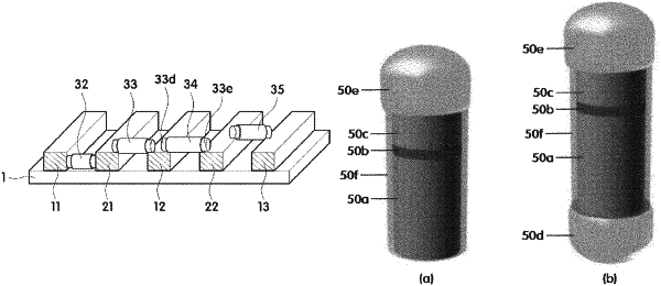
1. A light-emitting element comprising:
a first semiconductor layer;
a second semiconductor layer;
an active layer between the first semiconductor layer and the second semiconductor layer; and
an electrode layer directly on at least one of the first semiconductor layer or the second semiconductor layer,
wherein the electrode layer comprises a first surface contacting the first semiconductor layer or the second semiconductor layer, and a second surface opposite the first surface, and
wherein the second surface has a curved portion in one direction in which the first semiconductor layer, the active layer, and the second semiconductor layer are arranged, wherein the light-emitting element extends in the one direction, the curved portion terminating at a location adjacent to one of the first semiconductor layer or the second semiconductor layer that contacts the first surface of the electrode layer.
|