| CPC H01L 31/024 (2013.01) [H01L 25/10 (2013.01); H01L 25/105 (2013.01); H01L 25/11 (2013.01); H01L 25/18 (2013.01); H01L 25/50 (2013.01); H01L 27/14 (2013.01); H01L 27/1469 (2013.01); H01L 27/14618 (2013.01); H01L 27/14625 (2013.01); H01L 27/14627 (2013.01); H01L 27/14634 (2013.01); H01L 27/14636 (2013.01); H01L 31/0203 (2013.01); H01L 31/0224 (2013.01); H04N 23/54 (2023.01); H04N 23/55 (2023.01); H01L 2224/16225 (2013.01); H01L 2225/1017 (2013.01); H01L 2225/1058 (2013.01); H01L 2225/1094 (2013.01)] | 9 Claims |
|
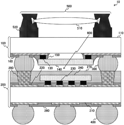
1. A semiconductor device, comprising:
a first package that includes:
a first substrate;
a first semiconductor chip configured to output a signal, wherein the first semiconductor chip is below the first substrate;
a first wiring electrically connected to the first semiconductor chip through a metal bump, wherein the first wiring is below the first substrate; and
a first protective film that includes a first opening portion;
a second package that includes:
a second substrate;
a second semiconductor chip configured to process the signal output from the first semiconductor chip, wherein the second semiconductor chip is above the second substrate;
a second wiring electrically connected to the second semiconductor chip, wherein the second wiring is on each of a front surface of the second substrate and a back surface of the second substrate;
an encapsulant configured to seal the second semiconductor chip and a conductive member in an opening in the encapsulant, wherein the first semiconductor chip faces the encapsulant in a non-contact manner and a gap is defined between the first semiconductor chip and the encapsulant to be 0.05 mm; and
a second protective film that includes a second opening portion, wherein the second protective film is on each of the front surface of the second substrate and the back surface of the second substrate;
a first connection portion configured to electrically connect the first wiring and the second wiring; and
a second connection portion electrically connected to the second wiring, wherein
the first protective film is in contact with each of the first connection portion, the first wiring, and the first substrate,
the first connection portion is in contact with the first wiring via the first opening portion, and
the second connection portion is in contact with the second wiring via the second opening portion.
|