| CPC H01L 31/022425 (2013.01) [H01L 31/0201 (2013.01); H01L 31/02167 (2013.01); H01L 31/0504 (2013.01); H01L 31/0508 (2013.01); Y02E 10/50 (2013.01)] | 18 Claims |
|
1. A solar cell panel comprising:
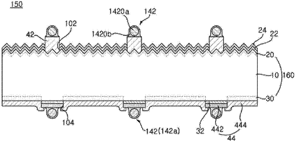
a plurality of solar cells; and a wire for interconnecting two neighboring solar cells among the solar cells, the wire having a circular core and a solder layer surrounding the circular core,
wherein each of the solar cells includes:
a semiconductor substrate;
a first electrode formed on a first surface of the semiconductor substrate;
a second electrode formed on a second surface of the semiconductor substrate;
a second pad electrode connected to the second electrode,
wherein the second electrode and the second pad electrode are spaced apart from each other in a first direction so as to form a gap portion therebetween such that the second electrode and the second pad electrode define the gap portion,
wherein the second electrode and the second pad electrode overlap each other in a second direction crossing the first direction,
wherein the wire includes a first portion disposed on the second pad electrode and a second portion disposed on the gap portion or the second electrode,
wherein a distance between the second portion of the wire disposed on the second electrode and the substrate is gradually reduced over the gap portion until the first portion of the wire comes in contact with the second pad electrode,
wherein a width of the first portion is greater than a width of the second portion by soldering the solder layer on the second pad electrode,
wherein the width of the first portion is smaller than a width of the second pad electrode, and the width of the second portion is smaller than a width of the gap portion in the second direction, and
wherein an overlap portion is formed on each of both sides of the second pad electrode in the second direction along both sides of the gap portion in a rectangular shape having a same length as the second pad electrode in the first direction, and each of the overlap portions that are formed on each of the both sides of the second pad electrode having a same width in the second direction; and
a passivation film directly disposed on the second surface of the semiconductor substrate,
wherein the passivation film is locally formed so as to correspond to only an area defined by the second pad electrode and the gap portion such that the passivation film is between the second surface of the semiconductor substrate and a surface defined by the second pad electrode and the gap portion and in direct contact with the surface defined by the second pad electrode and the gap portion, and
wherein a side surface of the passivation film is in direct contact with the second electrode.
|