| CPC H01L 29/872 (2013.01) [H01L 29/0607 (2013.01); H01L 29/1608 (2013.01)] | 8 Claims |
|
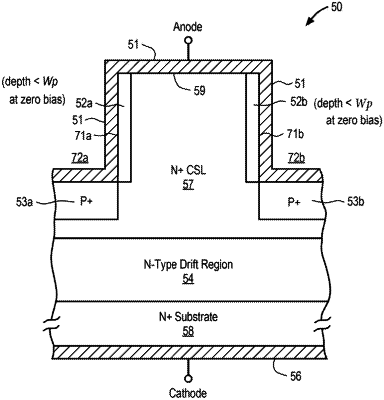
1. A Junction Barrier Schottky (JBS) diode comprising: a silicon carbide (SiC) substrate of a first conductivity type;
an upper region having a first doping concentration of a first conductivity type, the upper region being disposed above the SiC substrate, the upper region having a top portion defined as a mesa by first and second trenches, the mesa having first and second sidewalls and a top planar surface;
first and second shallow layers of a second conductivity type disposed in the mesa respectively adjoining the first and second sidewalls, each of the first and second shallow layers extending vertically along the first and second sidewalls, respectively, the first and second shallow layers each having a lateral thickness and a second doping concentration, the lateral thickness being less than a width of a depletion region in each of the first and second shallow layers such that the first and second shallow layers are completely depleted at a zero bias condition of the JBS diode;
a top metal layer disposed along the top planar surface, the first and second sidewalls, and a bottom of each of the first and second trenches, the top metal layer being in direct contact with a central portion of the upper region that extends to the top planar surface, the top metal layer comprising an anode of the JBS diode;
first and second deep regions of the second conductivity type, the first and second deep regions being disposed in the upper region directly beneath and adjoining the bottom of the first and second trenches, respectively, the first and second deep regions extending downward to a vertical depth substantially greater than the thickness of the shallow layer, the first and second deep regions being laterally spaced-apart, each of the first and second deep regions having a third doping concentration substantially greater than the second doping concentration, the top metal layer being in direct contact with the first and second deep regions; and a bottom metal layer disposed beneath the SiC substrate, the bottom metal layer comprising a cathode of the JBS diode.
|