| CPC H01L 29/7881 (2013.01) [H01L 29/40114 (2019.08); H01L 29/42332 (2013.01); H01L 29/66825 (2013.01)] | 9 Claims |
|
1. A split-gate memory device, comprising:
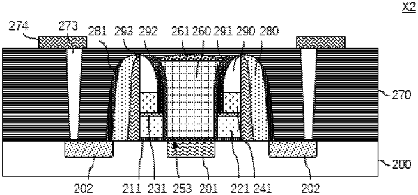
a substrate, having a memory cell region comprising a connecting subregion and a functional subregion;
first and second gate structures provided in the memory cell region, each of the first and second gate structures comprising a floating gate above the substrate, an inter-gate dielectric layer on the floating gate and a control gate on the inter-gate dielectric layer, the second gate structure being mirrored to the first gate structure;
a source region provided in the substrate between the first and second gate structures; and
electrical connections, including a first electrical connection region and a second electrical connection region separate from the first electrical connection region,
wherein in the connecting subregion, the first electrical connection region connects the control gate, the second electrical connection region connects the source region, and the first electrical connection region is electrically connected to the second electrical connection region,
wherein each of the first and second gate structures further comprises a first spacer and a second spacer, the first spacer residing on the inter-gate dielectric layer and covering a side of the control gate close to the source region, the second spacer residing on the substrate and covering a side of each of the first spacer, the control gate and the inter-gate dielectric layer close to the source region,
wherein each of the first and second gate structures further comprises a third spacer which covers a side of each of the floating gate, the inter-gate dielectric layer and the control gate away from the source region, and
wherein in the functional subregion, a protective layer is provided on the control gate of each of the first and second gate structures, the protective layer being in a shape of a wedge having a vertical surface away from the source region and a bevel surface close to the source region, the bevel surface covered partially by the first spacer and partially by the second spacer, the vertical surface covered by the third spacer.
|