| CPC H01L 29/7869 (2013.01) [H01L 27/1225 (2013.01); H01L 29/04 (2013.01); H01L 29/045 (2013.01); H01L 29/24 (2013.01); H01L 29/66969 (2013.01); H01L 29/78648 (2013.01); H01L 29/78693 (2013.01); H01L 29/78696 (2013.01)] | 4 Claims |
|
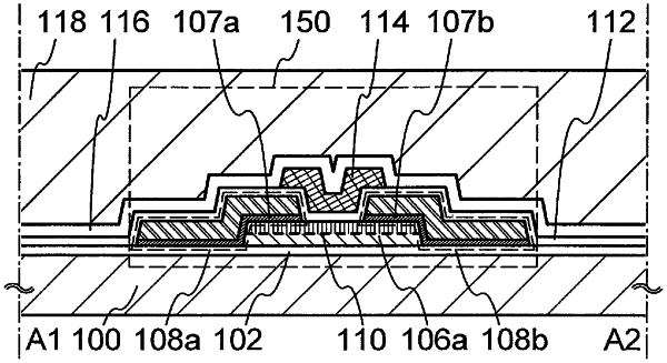
1. A semiconductor device comprising:
a first insulating layer;
an oxide semiconductor layer including a channel formation region of a transistor, over the first insulating layer;
a source electrode and a drain electrode in contact with the oxide semiconductor layer; and
a second insulating layer having a region in contact with a top surface of the source electrode, a top surface of the drain electrode and a top surface of the oxide semiconductor layer,
wherein the source electrode includes a first conductive layer over and in contact with the oxide semiconductor layer, and a second conductive layer over and in contact with the first conductive layer,
wherein the drain electrode includes a third conductive layer over and in contact with the oxide semiconductor layer, and a fourth conductive layer over and in contact with the first conductive layer,
wherein a thickness of the first conductive layer is smaller than a thickness of the second conductive layer,
wherein a thickness of the third conductive layer is smaller than a thickness of the fourth conductive layer,
wherein the oxide semiconductor layer includes indium, gallium and zinc,
wherein the oxide semiconductor layer has a region overlapping with the second insulating layer without overlapping with the source electrode or the drain electrode,
wherein the oxide semiconductor layer has a first region including a crystal whose c-axis is aligned, a second region in contact with the source electrode or the drain electrode, and a third region in contact with the first insulating layer,
wherein each of the second region and the third region has a different crystallinity from the first region, and
wherein the first region is provided over the third region.
|