| CPC H01L 29/7855 (2013.01) [H01L 21/02532 (2013.01); H01L 21/76871 (2013.01); H01L 21/823431 (2013.01); H01L 27/0886 (2013.01); H01L 29/0847 (2013.01); H01L 29/165 (2013.01); H01L 29/4232 (2013.01); H01L 29/6656 (2013.01); H01L 29/66795 (2013.01); H01L 29/785 (2013.01); H01L 21/02645 (2013.01); H01L 27/1211 (2013.01); H01L 29/4966 (2013.01); H01L 29/66545 (2013.01)] | 12 Claims |
|
1. A semiconductor device comprising:
a substrate;
a first fin type pattern disposed on the substrate;
a second fin type pattern disposed on the substrate;
a field insulation disposed on the substrate, and disposed between the first fin type pattern and the second fin type pattern;
a first gate disposed on the first fin type pattern, the second fin type pattern, and the field insulation;
a second gate disposed on the first fin type pattern, the second fin type pattern, and the field insulation; and
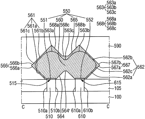
an epitaxial pattern disposed on the first fin type pattern and the second fin type pattern, the epitaxial pattern being included in a source/drain of a transistor,
wherein the epitaxial pattern includes:
a shared semiconductor pattern disposed on the first fin type pattern and the second fin type pattern, the shared semiconductor pattern including a curved top surface and curved sidewall surfaces, and
a capping semiconductor pattern disposed directly on the curved top surface and on the curved sidewall surfaces of the shared semiconductor pattern, the capping semiconductor pattern having a varying width, and an upper surface of the capping semiconductor pattern including a recess that includes a linear connecting portion that is parallel to a bottom of the substrate, and
wherein the capping semiconductor pattern is a single layer.
|