| CPC H01L 29/7849 (2013.01) [H01L 21/76224 (2013.01); H01L 29/785 (2013.01)] | 20 Claims |
|
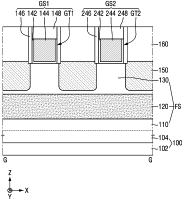
1. A semiconductor device comprises:
a substrate;
a fin structure on the substrate;
a field insulation layer on a sidewall portion of the fin structure; and
a gate electrode on the fin structure, the gate electrode intersecting the fin structure,
wherein the fin structure includes a first semiconductor pattern, a stress pattern, and a second semiconductor pattern that are sequentially stacked on the substrate,
wherein the stress pattern comprises an oxide including germanium, and
wherein a first angle between an upper surface of the first semiconductor pattern and a first line parallel to an upper surface of the substrate is different from a second angle between a lower surface of the second semiconductor pattern and a second line parallel to the upper surface of the substrate.
|