| CPC H01L 29/7848 (2013.01) [H01L 21/28167 (2013.01); H01L 21/76264 (2013.01); H01L 29/0895 (2013.01); H01L 29/66621 (2013.01); H01L 29/66628 (2013.01); H01L 29/66636 (2013.01); H01L 29/66651 (2013.01); H01L 29/785 (2013.01); H01L 29/7833 (2013.01)] | 18 Claims |
|
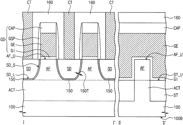
1. A method of manufacturing a semiconductor device, the method comprising:
forming at least one active pattern on a substrate;
forming at least one gate electrode intersecting the at least one active pattern;
forming recesses in the at least one active pattern, the recesses being on opposite sides of the at least one gate electrode;
conformally forming a barrier layer in at least one of the recesses, such that the barrier layer includes oxygen and has a thickness of about 2 angstroms to about 5 angstroms; and
forming source/drain regions through the barrier layer by epitaxially growing the source/drain regions using the at least one active pattern as a seed layer.
|