| CPC H01L 29/7816 (2013.01) [H01L 29/66295 (2013.01); H01L 29/7395 (2013.01)] | 16 Claims |
|
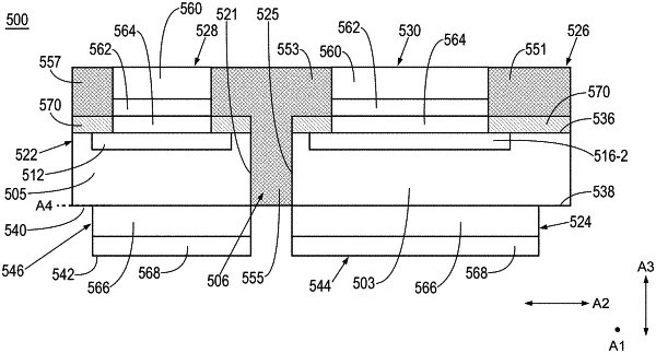
1. A semiconductor device for integrating multiple transistors, the semiconductor device comprising:
a wafer substrate including a first region and a second region, the first region defining at least a portion of at least one first transistor, the second region defining at least a portion of at least one second transistor;
an isolation area located between the first region and the second region;
at least one terminal of the at least one first transistor contacting the first region of the wafer substrate;
at least one terminal of the at least one second transistor contacting the second region of the wafer substrate;
an electrode coupled to the at least one terminal of the at least one first transistor; and
an encapsulation material, the encapsulation material including a first portion located within the isolation area and a second portion extending from the first portion to at least a portion of a first edge of the electrode, the encapsulation material including a third portion that extends between a second edge of the electrode and an edge of the semiconductor device.
|